Address
304 North Cardinal
St. Dorchester Center, MA 02124
Work Hours
Monday to Friday: 7AM - 7PM
Weekend: 10AM - 5PM
Address
304 North Cardinal
St. Dorchester Center, MA 02124
Work Hours
Monday to Friday: 7AM - 7PM
Weekend: 10AM - 5PM
Brief introduction of z490 motherboard workflow
Maintenance process:
1. Before the power supply is plugged in, the 3V button battery is converted to the RTC circuit VCC of the bridge through the circuit.
2. The 3V battery provides high-level rtcrst to the bridge after circuit conversion and CMOS cap hopping#.
3. The bridge vibrates Crystal,VCC and Crystal, and generates 32.768KHz to the bridge.
4. Insert ATX and output 5VSB with purple line.
5. 5VSB is usually converted by voltage regulator to generate 3.3V deep sleep standby VCC for IO and Bridge (vccdsw ﹤ 3p3).
After IO detects that VCC is normal, it sends out deep sleep standby VCC good to bridge (DSW? Pwrok).
Bridge sends SLP_Sus ා control to generate the main standby VCC(vccprim š 3p3, vccprim Ŧ 1p8, vccprim ා 1p05).
The 3.3V main standby VCC supplies the PCIe slot, network card, IO and bridge.
The bridge reads BIOS and configures pin bit.
6. Generally, after IO detects that the standby VCC is normal, it sends the standby VCC good (rsmrst ා) to the bridge.
7.switch,Switch, incoming IO.
8. IO sends a power on request signal to the bridge (pwrbtn ා).
9. Bridge sends signal SLP_S *, where SLP_S3 to IO.
Or the bridge sends the signal of allowing you to start the machine to IO through the ESPI bus.
10. IO lowers the green line of ATX (pson ා).
VCC tart-up mode of ESPI is allowed, all channels of ESPI will send out signals.
11. Power output 12V / 5V / 3.3V / – 12V.
12、SLP_S4 ා first control the generation of vpp2.5v and ᦇ 1.05v ᦇ vccstpll, and then convert control to generate main memory VCC 1.2v.
13、SLP_S3 ා controls the generation of 1.05v vccstg.
SLP_After S3 ා and memory VCC are normal, the control generates 0.95v vccio VCC and 1.05v vccsa VCC.
14. After the above VCC is normal, the conversion generates EN of CPU VCC.
But it will not generate CPU VCC, vboot = 0V.
15. CPU VCC chip sends signal to PCH of bridge_Pwrok, indicating that the chip is ready to generate CPU VCC.
16. The PG of gray line is sent to IO by ATX power delay.
17. After IO detects that VCC and atxpg are normal, it sends PG to sys of bridge_PWROK.
18. 24m starting vibration of bridge.
19. The bridge sends CLK signal and cpupwrgd to CPU.
20. Bridge sends platform reset pltrst to IO, IO sends reset to network card, PCIe, etc.
21. The bridge sends out the reset CPU of CPU_RST#.
CPU sends SVID signal to CPU chip VCC.
CPU VCC chip control output CPU VCC/ adjust CPU VCC to a value suitable for the current CPU.
Start to read the CPU and run the BIOS code.
After z490 self checks the memory, the CPU sends out the second SVID and controls the generation of centralized display VCC vccg.
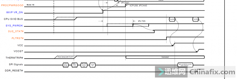
Z490 motherboard workflow introduction Figure 1.