Address
304 North Cardinal
St. Dorchester Center, MA 02124
Work Hours
Monday to Friday: 7AM - 7PM
Weekend: 10AM - 5PM
Address
304 North Cardinal
St. Dorchester Center, MA 02124
Work Hours
Monday to Friday: 7AM - 7PM
Weekend: 10AM - 5PM
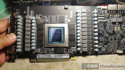
= = About the transformation test of the burning defect of the graphics card = =
If there is a graphics card, PCB VCC is burned, and the most important phase 1 and phase 2 are burned, and the area is very large, can this PCB still be saved? As shown in the figure:
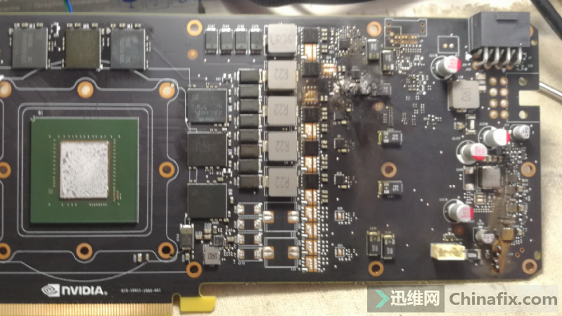
About the transformation test of the burning defect of the graphics card Figure 1.
This 1070 VCC, the core of the first and second phases, is burned, and the burned area is relatively large. If mining, including the driver IC, the 100UF Capacitor on the side, the first phase composite pipe should be dug up.
As the first phase and the second phase are the necessary phases (9511p white paper says that if ISEN pin is pulled to a high potential of 5V, the phase will be turned off. However, when the PWM is turned off successively, that is, 7-8 phases are turned off, it will work in 1-6 phases, and 5-6-7-8 phases will work in 1-4 phases. But you can’t turn off the 1~2 phases, and let the back 345678 work). If the 1~2 phases are missing, then even if the 5~6 phases are completed, it’s hard to say whether the core VCC and 9511p can work normally, but the square wave of the missing two phases on the time axis, the accuracy and ripple of VCC and the current following performance of VCC will definitely decline.
So, is there any way to make up the first to second phases? There are two options:
Scheme 1: install the driver IC with a small driver IC board and then Jump wire, or directly install the driver IC on the half PAD on the side of the dug pit and then Jump wire. Because of the poor reliability of Jump wire and its operation at the edge of the dug pit, it always feels unreliable.
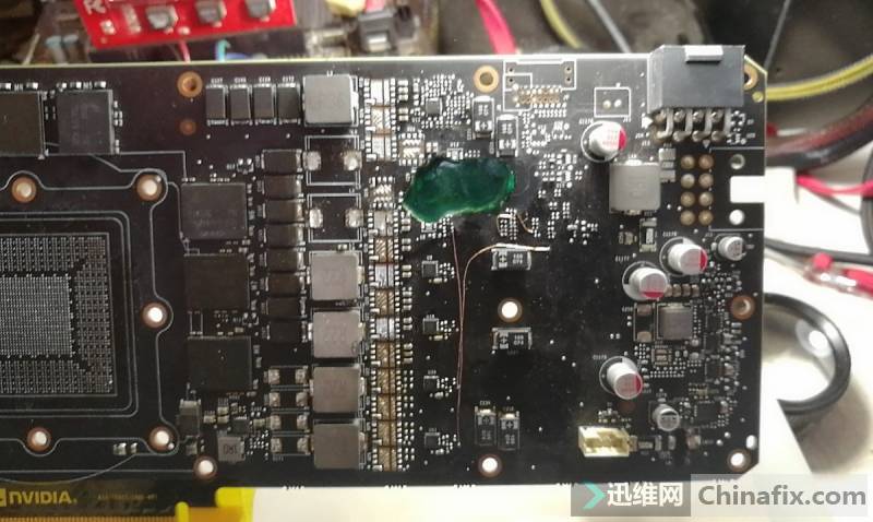
Scheme 2: Observing Boardview, it is found that the 5th ~ 6th phases can actually be changed to 1st ~ 2nd phases, as long as the input of ISEN pin is changed from ISEN1,6 to 9511P to input 2. Change the PWM output accordingly. Then change some small components of Inductor FB PH signal. You can basically transplant these two phases.
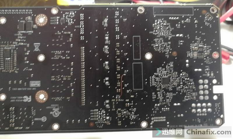
Option two, just do it. First, fill the 5~6 two-phase components (install the composite pipes separately first). All ISEN pin of 9511P is led out to the circuit of driving IC FB by a 2K resistor. After research, two ISEN5~6 signals of 1070 are directly pulled up by 5V, directly from the front of the card PH1 Jump wire PH5,PH2 Jump wire PH6, And move four resistors (20K*2 1 Euro *2), then Jump wire PWM1 to drive ICPWM5 solder joint, fly PWM2 to PWM6 solder joint (the original PWM1~2 is basically empty on PCB because all components such as driver IC and composite are removed, so there is no need to deal with it), and make up necessary peripheral components such as VCC resistor of driver IC, vibration damping circuit, etc.
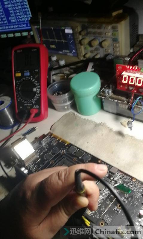
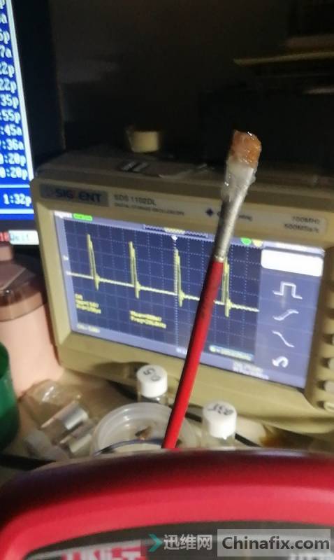
When the composite pipe is not installed, power on to see if the driver IC sends out a test square wave, and the measured four paths all send out test waves normally.
Then, install the composite pipe, and connect the core dummy load (the core Move Board (move the main chips to another motherboard)has been removed, so find a high-power 1 ohm resistor as the dummy load). After power-on, the measured waveform of PWM VCC with 5~6 two-phase transformation is normal, and the measured core VCC 0.83V is normal.
Transformation successful!
About the transformation test of the burning defect of the graphics card Figure 2.
About the transformation test of the burning defect of the graphics card Figure 3.
About the transformation test of the burning defect of the graphics card Figure 4.
About the transformation test of the burning defect of the graphics card Figure 5.
Summary: This transformation has no practical significance. Now the card is cheap, and there is not much money for a backplane. But theoretically, it can be transformed in this way. Of course, there are disadvantages, that is, the first phase of the golden finger 12V VCC must be good by default, otherwise, if you dial 8 pins to connect VCC externally, the power-on core can’t work without the default VCC, so you can’t send out the prompt that the cable is unplugged. That is to say, 8 pins must be.